- 您現(xiàn)在的位置:買賣IC網(wǎng) > PDF目錄359072 > M5451Q (意法半導體) LED DISPLAY DRIVERS PDF資料下載
參數(shù)資料
| 型號: | M5451Q |
| 廠商: | 意法半導體 |
| 英文描述: | LED DISPLAY DRIVERS |
| 中文描述: | LED顯示驅動器 |
| 文件頁數(shù): | 3/8頁 |
| 文件大?。?/td> | 142K |
| 代理商: | M5451Q |
At the low state of the clock a RESET signal is
generated which clears all the shift registers for the
next set of data. The shift registers are static mas-
ter-slave configurations. There is no clear for the
master portion of the first shift register, thus allow-
ing continuous operation.
There must be a complete set of 36 clocks or the
shift registers will not clear.
When power is first applied to the chip an internal
power ON reset signal is generated which resets
all registers and all latches. The START bit and the
first clock return the chip to its normal operation.
Bit 1 is the first bit following the start bit and it will
appear on Pin 18. A logical "1" at the input will turn
on the appropriate LED.
Figure 3 shows the timing relationship between
Data, Clock and DATA ENABLE.
A max clock frequency of 0.5MHz is assumed.
For applications where a lesser number of outputs
are used, it is possible to either increase the current
per output or operate the part at higher than 1V
V
OUT
.
The following equation can be used for calcula-
tions.
T
j
= [(V
OUT
) (I
LED
) (No. of segments) + (V
DD
7mA)]
(124
°
C/W) + T
amb
where :
T
j
= junction temperature (150
°
C max)
V
OUT
= the voltage at the LED driver outputs
I
LED
= the LED current
124
°
C/W = thermal coefficient of the package
T
amb
= ambient temperature
The above equation was used to plot Figures 4, 5
and 6.
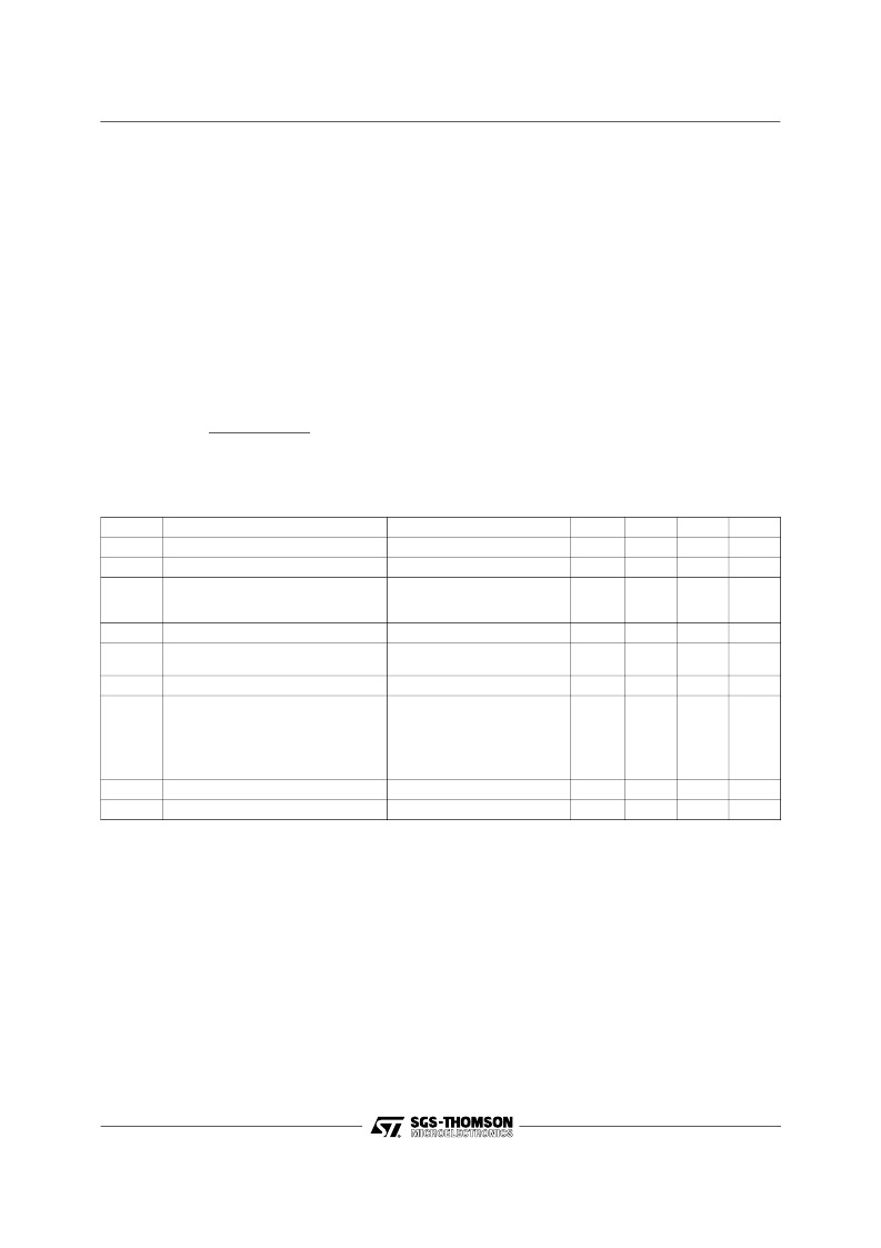
STATIC ELECTRICAL CHARACTERISTICS
(T
amb
within operating range, V
DD
= 4.75V to 13.2V, V
SS
= 0V, unless otherwise specified)
Symbol
V
DD
I
DD
V
I
Parameter
Test Conditions
Min.
4.75
Typ.
Max.
13.2
7
0.8
V
DD
V
DD
0.75
4.3
Unit
V
mA
V
V
V
mA
V
Supply Voltage
Supply Current
Input Voltage
V
DD
= 13.2V
±
10
μ
A Input Bias
4.75
≤
V
≤
5.25
V
DD
> 5.25
Logical "0" Level
Logical "1" Level
- 0.3
2.2
V
DD
- 2
0
3
I
B
V
B
Brightness
Input
Current
(note
2)
Brightness
Input
Voltage
(pin
19)
Input Current = 750
μ
A,
T
amb
= 25
C
V
O(off)
I
O
Off State Out. Voltage
Out. Sink Current (note 3)
13.2
V
Segment OFF
Segment ON
V
O
= 3V
V
O
= 1V (note 4)
Brightness In. = 0
μ
A
Brightness In. = 100
μ
A
Brightness In. = 750
μ
A
0
2
12
0
2.7
15
10
10
4
25
0.5
±
20
μ
A
μ
A
mA
mA
MHz
%
f
clock
I
O
Input Clock Frequency
Output Matching (note 1)
5
Notes :
1. Output matching is calculated as the percent variation from I
+ I
/2.
2. With a fixed resistor on the brightness input some variation in brightness will occur from one device to another.
3. Absolute maximum for each output should be limited to 40mA.
4. The V
O
voltage should be regulated by the user. See figures 5 and 6 for allowable V
O
versus I
O
operation.
M5450 - M5451
3/8
相關PDF資料 |
PDF描述 |
|---|---|
| M5480 | LED DISPLAY DRIVER |
| M5480B7 | LED DISPLAY DRIVER |
| M5481 | LED DISPLAY DRIVER |
| M5481B7 | LED DISPLAY DRIVER |
| M5482 | CAP 36D SERIES, |
相關代理商/技術參數(shù) |
參數(shù)描述 |
|---|---|
| M5451QT | 功能描述:LED顯示驅動器 LED DISPLAY DRIVER RoHS:否 制造商:Micrel 數(shù)位數(shù)量:5 片段數(shù)量: 安裝風格:SMD/SMT 封裝 / 箱體:PLCC-44 工作電源電壓:4.75 V to 11 V 最大電源電流:10 mA 最大工作溫度:+ 85 C 最小工作溫度:- 40 C 封裝:Tube |
| M54521P | 制造商:MITSUBISHI 制造商全稱:Mitsubishi Electric Semiconductor 功能描述:5-UNIT 500MA DARLINGTON TRANSISTOR ARRAY |
| M54522FP | 制造商:MITSUBISHI 制造商全稱:Mitsubishi Electric Semiconductor 功能描述:8-UNIT 400mA DARLINGTON TRANSISTOR ARRAY WITH CLAMP DIODE |
| M54522FP-200D | 制造商:Powerex Power Semiconductors 功能描述: 制造商:PWRX 功能描述: |
| M54522P | 制造商:MITSUBISHI 制造商全稱:Mitsubishi Electric Semiconductor 功能描述:8-UNIT 400mA DARLINGTON TRANSISTOR ARRAY WITH CLAMP DIODE |
發(fā)布緊急采購,3分鐘左右您將得到回復。