- 您現(xiàn)在的位置:買(mǎi)賣(mài)IC網(wǎng) > PDF目錄359067 > M48Z08-100MH6 (意法半導(dǎo)體) 64 Kbit 8Kb x 8 ZEROPOWER SRAM PDF資料下載
參數(shù)資料
| 型號(hào): | M48Z08-100MH6 |
| 廠商: | 意法半導(dǎo)體 |
| 英文描述: | 64 Kbit 8Kb x 8 ZEROPOWER SRAM |
| 中文描述: | 64千位的8kB × 8 ZEROPOWER的SRAM |
| 文件頁(yè)數(shù): | 7/18頁(yè) |
| 文件大?。?/td> | 141K |
| 代理商: | M48Z08-100MH6 |
第1頁(yè)第2頁(yè)第3頁(yè)第4頁(yè)第5頁(yè)第6頁(yè)當(dāng)前第7頁(yè)第8頁(yè)第9頁(yè)第10頁(yè)第11頁(yè)第12頁(yè)第13頁(yè)第14頁(yè)第15頁(yè)第16頁(yè)第17頁(yè)第18頁(yè)
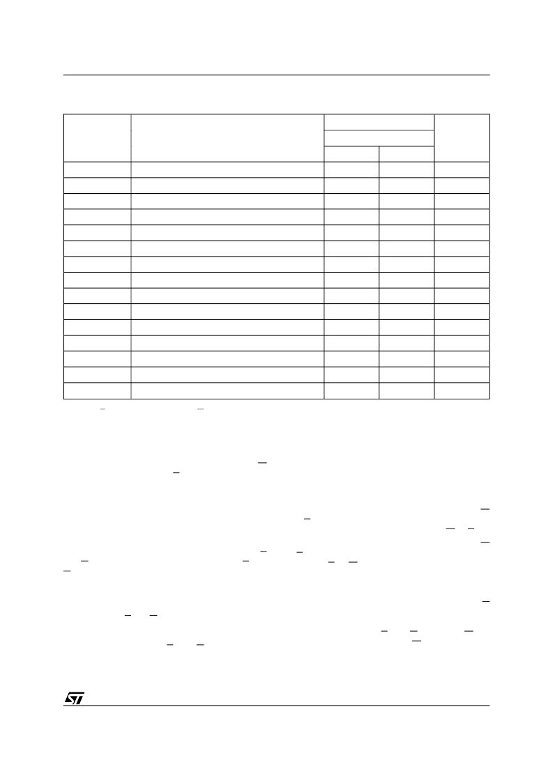
Symbol
Parameter
M48Z08 / M48Z18
Unit
-100
Min
Max
t
AVAV
Write Cycle Time
100
ns
t
AVWL
Address Valid to Write Enable Low
0
ns
t
AVEL
Address Valid to Chip Enable Low
0
ns
t
WLWH
Write Enable Pulse Width
80
ns
t
ELEH
Chip Enable Low to Chip Enable High
80
ns
t
WHAX
Write Enable High to Address Transition
10
ns
t
EHAX
Chip Enable High to Address Transition
10
ns
t
DVWH
Input Valid to Write Enable High
50
ns
t
DVEH
Input Valid to Chip Enable High
30
ns
t
WHDX
Write Enable High to Input Transition
5
ns
t
E1HDX
Chip Enable High to Input Transition
5
ns
t
WLQZ (1, 2)
Write Enable Low to Output Hi-Z
50
ns
t
AVWH
Address Valid to Write Enable High
80
ns
t
AVEH
Address Valid to Chip Enable High
80
ns
t
WHQX (1, 2)
Write Enable High to Output Transition
10
ns
Notes:
1. C
= 30pF (see Figure 4).
2. If E goes low simultaneously with W going low, the outputs remain in the high impedance state.
Table 10. Write Mode AC Characteristics
(T
A
= 0 to 70
°
C; V
CC
= 4.75V to 5.5V or 4.5V to 5.5V)
READ MODE
The M48Z08/18 is in the Read Mode whenever W
(Write Enable) is high and E (Chip Enable) is low.
The device architecture allows ripple-through ac-
cess of data from eight of 65,536 locations in the
static storage array. Thus, the unique address
specified by the 13 Address Inputs defines which
one of the 8,192 bytes of data is to be accessed.
Valid data will be available at the Data I/O pins
within Address Access time (t
AVQV
) after the last
address input signal is stable, providing that the E
and G access times are also satisfied. If the E and
G access times are not met, valid data will be
available after the latter of the Chip Enable Access
time (t
ELQV
) or Output Enable Access time (t
GLQV
).
The state of the eight three-state Data I/O signals
is controlled by E and G. If the outputs are activated
before t
AVQV
, the data lines will be driven to an
indeterminate state until t
AVQV
. If the Address In-
puts are changed while E and G remain active,
output data will remain valid for Output Data Hold
time (t
AXQX
) but will go indeterminate until the next
Address Access.
WRITE MODE
The M48Z08/18 is in the Write Mode whenever W
and E are active. The start of a write is referenced
from the latter occurring falling edge of W or E.
A write is terminated by the earlier rising edge of W
or E. The addresses must be held valid throughout
the cycle. E or W must return high for a minimum
of t
EHAX
from Chip Enable or t
WHAX
from Write
Enable prior to the initiation of another read or write
cycle. Data-in must be valid t
DVWH
prior to the end
of write and remain valid for t
WHDX
afterward. G
should be kept high during write cycles to avoid bus
contention; although, if the output bus has been
activated by a low on E and G, a low on W will
disable the outputs t
WLQZ
after W falls.
7/18
M48Z08, M48Z18
相關(guān)PDF資料 |
PDF描述 |
|---|---|
| M48Z08-100MH1TR | 64 Kbit 8Kb x 8 ZEROPOWER SRAM |
| M48Z08PC | 64 Kbit 8Kb x 8 ZEROPOWER SRAM |
| M48Z08MH | 64 Kbit 8Kb x 8 ZEROPOWER SRAM |
| M48Z128YSH | Hook-Up Wire; Conductor Size AWG:24; No. Strands x Strand Size:Solid; Jacket Color:Green; Approval Bodies:UL, CSA; Approval Categories:UL AWM Style 1061; CSA AWM; Conductor Material:Copper; Jacket Material:Polyvinylchloride (PVC) RoHS Compliant: Yes |
| M48Z128Y-85CS1 | PADLOCK STN W/ 5 STEEL PADLOCKS |
相關(guān)代理商/技術(shù)參數(shù) |
參數(shù)描述 |
|---|---|
| M48Z08-100MH6TR | 制造商:STMICROELECTRONICS 制造商全稱(chēng):STMicroelectronics 功能描述:CMOS 8K x 8 TIMEKEEPER SRAM |
| M48Z08-100PC1 | 功能描述:NVRAM 64K (8Kx8) 100ns RoHS:否 制造商:Maxim Integrated 數(shù)據(jù)總線寬度:8 bit 存儲(chǔ)容量:1024 Kbit 組織:128 K x 8 接口類(lèi)型:Parallel 訪問(wèn)時(shí)間:70 ns 電源電壓-最大:5.5 V 電源電壓-最小:4.5 V 工作電流:85 mA 最大工作溫度:+ 70 C 最小工作溫度:0 C 封裝 / 箱體:EDIP 封裝:Tube |
| M48Z08-100PC1 | 制造商:STMicroelectronics 功能描述:ZEROPOWER SRAM 64K 48Z08 DIP28 |
| M48Z08-100PC1TR | 制造商:STMICROELECTRONICS 制造商全稱(chēng):STMicroelectronics 功能描述:5V, 64 Kbit (8Kb x 8) ZEROPOWER㈢ SRAM |
| M48Z08-100PC6 | 制造商:STMicroelectronics 功能描述: |
發(fā)布緊急采購(gòu),3分鐘左右您將得到回復(fù)。