- 您現(xiàn)在的位置:買(mǎi)賣(mài)IC網(wǎng) > PDF目錄358866 > LM4732TA (NATIONAL SEMICONDUCTOR CORP) Stereo 50W Audio Power Amplifier with Mute PDF資料下載
參數(shù)資料
| 型號(hào): | LM4732TA |
| 廠商: | NATIONAL SEMICONDUCTOR CORP |
| 元件分類(lèi): | 音頻/視頻放大 |
| 英文描述: | Stereo 50W Audio Power Amplifier with Mute |
| 中文描述: | 50 W, 2 CHANNEL, AUDIO AMPLIFIER, PZFM27 |
| 封裝: | PLASTIC, TO-220, 27 PIN |
| 文件頁(yè)數(shù): | 17/22頁(yè) |
| 文件大?。?/td> | 861K |
| 代理商: | LM4732TA |
第1頁(yè)第2頁(yè)第3頁(yè)第4頁(yè)第5頁(yè)第6頁(yè)第7頁(yè)第8頁(yè)第9頁(yè)第10頁(yè)第11頁(yè)第12頁(yè)第13頁(yè)第14頁(yè)第15頁(yè)第16頁(yè)當(dāng)前第17頁(yè)第18頁(yè)第19頁(yè)第20頁(yè)第21頁(yè)第22頁(yè)
Application Information
(Continued)
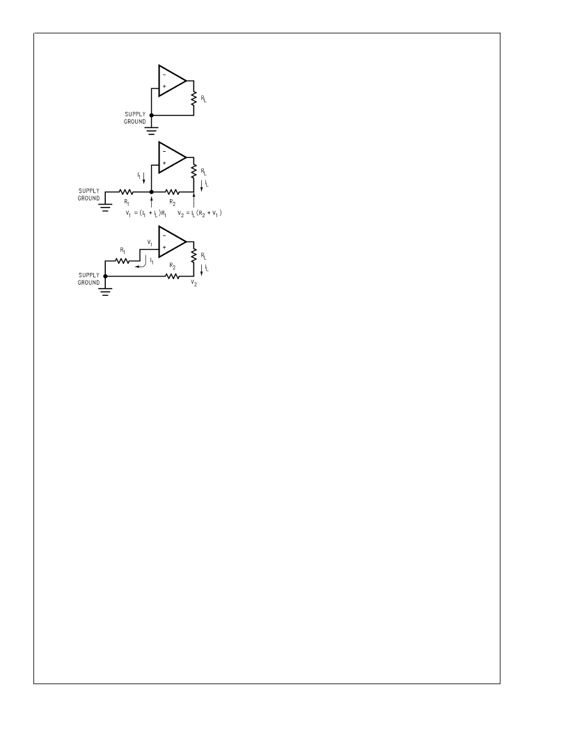
20072498
The load current I
L
will be much larger than input bias current
I
I
, thus V
1
will follow the output voltage directly, i.e. in phase.
Therefore the voltage appearing at the non-inverting input is
effectively positive feedback and the circuit may oscillate. If
there was only one device to worry about then the values of
R
and R
would probably be small enough to be ignored;
however, several devices normally comprise a total system.
Any ground return of a separate device, whose output is in
phase, can feedback in a similar manner and cause insta-
bilities. Out of phase ground loops also are troublesome,
causing unexpected gain and phase errors.
The solution to most ground loop problems is to always use
a single-point ground system, although this is sometimes
impractical. The third figure above is an example of a single-
point ground system.
The single-point ground concept should be applied rigor-
ously to all components and all circuits when possible. Vio-
lations of single-point grounding are most common among
printed circuit board designs, since the circuit is surrounded
by large ground areas which invite the temptation to run a
device to the closest ground spot. As a final rule, make all
ground returns low resistance and low inductance by using
large wire and wide traces.
Occasionally, current in the output leads (which function as
antennas) can be coupled through the air to the amplifier
input, resulting in high-frequency oscillation. This normally
happens when the source impedance is high or the input
leads are long. The problem can be eliminated by placing a
small capacitor, C
C
, (on the order of 50pF to 500pF) across
the LM4732 input terminals. Refer to the
External Compo-
nents Description
section relating to component interaction
with C
f
.
REACTIVE LOADING
It is hard for most power amplifiers to drive highly capacitive
loads very effectively and normally results in oscillations or
ringing on the square wave response. If the output of the
LM4732 is connected directly to a capacitor with no series
resistance, the square wave response will exhibit ringing if
the capacitance is greater than about 0.2μF. If highly capaci-
tive loads are expected due to long speaker cables, a
method commonly employed to protect amplifiers from low
impedances at high frequencies is to couple to the load
through a 10
resistor in parallel with a 0.7μH inductor. The
inductor-resistor combination as shown in the
Figure 5
iso-
lates the feedback amplifier from the load by providing high
output impedance at high frequencies thus allowing the 10
resistor to decouple the capacitive load and reduce the Q of
the series resonant circuit. The LR combination also pro-
vides low output impedance at low frequencies thus shorting
out the 10
resistor and allowing the amplifier to drive the
series RC load (large capacitive load due to long speaker
cables) directly.
INVERTING AMPLIFIER APPLICATION
The inverting amplifier configuration may be used instead of
the more common non-inverting amplifier configuration
shown in
Figure 1
. The inverting amplifier can have better
THD+N performance and eliminates the need for a large
capacitor (Ci) reducing cost and space requirements. The
values show in
Figure 6
are only one example of an amplifier
with a gain of 20V/V (Gain = -R
/R
). For different resistor
values, the value of R
B
should be eqaul to the parallel
combination of R
f
and Ri.
If the DC blocking input capacitor (C
) is used as shown, the
lower -3dB point is found using Equation (8) as discussed in
the
Proper Selection of External Components
section.
L
www.national.com
17
相關(guān)PDF資料 |
PDF描述 |
|---|---|
| LM4780 | Audio Power Amplifier Series Stereo 60W, Mono 120W Audio Power Amplifier with Mute |
| LM4780TA | Audio Power Amplifier Series Stereo 60W, Mono 120W Audio Power Amplifier with Mute |
| LM4781TA | Overture⑩ Audio Power Amplifier Series 3 Channel 35W Audio Power Amplifier with Mute |
| LM4781 | Overture⑩ Audio Power Amplifier Series 3 Channel 35W Audio Power Amplifier with Mute |
| LM4782TA | 3 Channel 25W Audio Power Amplifier with Mute and Standby |
相關(guān)代理商/技術(shù)參數(shù) |
參數(shù)描述 |
|---|---|
| LM4733 | 制造商:NSC 制造商全稱:National Semiconductor 功能描述:3 Channel 30W Audio Power Amplifier with Mute |
| LM4733BG240G320WCF | 制造商:DENSITRON 功能描述:LCD MODULE GRAPHIC |
| LM4733TA | 制造商:NSC 制造商全稱:National Semiconductor 功能描述:3 Channel 30W Audio Power Amplifier with Mute |
| LM4733TABD | 功能描述:音頻 IC 開(kāi)發(fā)工具 LM4733 EVAL BOARD RoHS:否 制造商:Texas Instruments 產(chǎn)品:Evaluation Kits 類(lèi)型:Audio Amplifiers 工具用于評(píng)估:TAS5614L 工作電源電壓:12 V to 38 V |
| LM4734 | 制造商:NSC 制造商全稱:National Semiconductor 功能描述:3 Channel 20W Audio Power Amplifier with Mute and Standby |
發(fā)布緊急采購(gòu),3分鐘左右您將得到回復(fù)。