- 您現(xiàn)在的位置:買賣IC網(wǎng) > PDF目錄358866 > LM4732TA (NATIONAL SEMICONDUCTOR CORP) Stereo 50W Audio Power Amplifier with Mute PDF資料下載
參數(shù)資料
| 型號: | LM4732TA |
| 廠商: | NATIONAL SEMICONDUCTOR CORP |
| 元件分類: | 音頻/視頻放大 |
| 英文描述: | Stereo 50W Audio Power Amplifier with Mute |
| 中文描述: | 50 W, 2 CHANNEL, AUDIO AMPLIFIER, PZFM27 |
| 封裝: | PLASTIC, TO-220, 27 PIN |
| 文件頁數(shù): | 14/22頁 |
| 文件大小: | 861K |
| 代理商: | LM4732TA |
Application Information
(Continued)
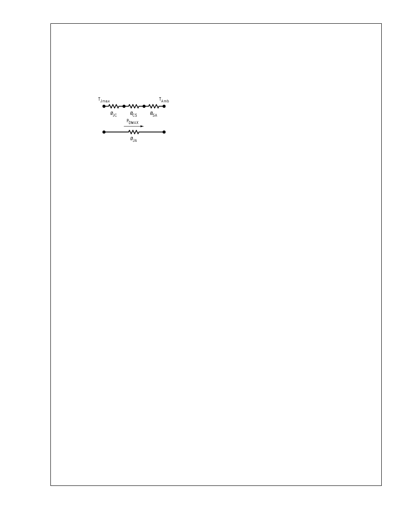
resistance is analogous to electrical resistance, and tem-
perature drops are analogous to voltage drops, the power
dissipation out of the LM4732 is equal to the following:
P
DMAX
= (T
JMAX
T
AMB
) /
θ
JA
(3)
where T
JMAX
= 150C, T
AMB
is the system ambient tempera-
ture and
JA
=
θ
JC
+
θ
CS
θ
SA
.
20072452
Once the maximum package power dissipation has been
calculated using
Equation (2)
, the maximum thermal resis-
tance,
θ
, (heat sink to ambient) in C/W for a heat sink can
be calculated. This calculation is made using
Equation (4)
which is derived by solving for
θ
SA
in
Equation (3)
.
θ
SA
= [(T
JMAX
T
AMB
)P
DMAX
(
θ
JC
+
θ
CS
)] / P
DMAX
(4)
Again it must be noted that the value of
θ
SA
is dependent
upon the system designer’s amplifier requirements. If the
ambient temperature that the audio amplifier is to be working
under is higher than 25C, then the thermal resistance for the
heat sink, given all other things are equal, will need to be
smaller.
SUPPLY BYPASSING
The LM4732 has excellent power supply rejection and does
not require a regulated supply. However, to improve system
performance as well as eliminate possible oscillations, the
LM4732 should have its supply leads bypassed with low-
inductance capacitors having short leads that are located
close to the package terminals. Inadequate power supply
bypassing will manifest itself by a low frequency oscillation
known as “motorboating” or by high frequency instabilities.
These instabilities can be eliminated through multiple by-
passing utilizing a large tantalum or electrolytic capacitor
(10μF or larger) which is used to absorb low frequency
variations and a small ceramic capacitor (0.1μF) to prevent
any high frequency feedback through the power supply lines.
If adequate bypassing is not provided, the current in the
supply leads which is a rectified component of the load
current may be fed back into internal circuitry. This signal
causes distortion at high frequencies requiring that the sup-
plies be bypassed at the package terminals with an electro-
lytic capacitor of 470μF or more.
BRIDGED AMPLIFIER APPLICATION
The LM4732 has two operational amplifiers internally, allow-
ing for a few different amplifier configurations. One of these
configurations is referred to as “bridged mode” and involves
driving the load differentially through the LM4732’s outputs.
This configuration is shown in
Figure 2
. Bridged mode op-
eration is different from the classical single-ended amplifier
configuration where one side of its load is connected to
ground.
A bridge amplifier design has a distinct advantage over the
single-ended configuration, as it provides differential drive to
the load, thus doubling output swing for a specified supply
voltage. Theoretically, four times the output power is pos-
sible as compared to a single-ended amplifier under the
same conditions. This increase in attainable output power
assumes that the amplifier is not current limited or clipped.
A direct consequence of the increased power delivered to
the load by a bridge amplifier is an increase in internal power
dissipation. For each operational amplifier in a bridge con-
figuration, the internal power dissipation will increase by a
factor of two over the single ended dissipation. Thus, for an
audio power amplifier such as the LM4732, which has two
operational amplifiers in one package, the package dissipa-
tion will increase by a factor of four. To calculate the
LM4732’s maximum power dissipation point for a bridged
load, multiply
Equation (2)
by a factor of four.
This value of P
can be used to calculate the correct size
heat sink for a bridged amplifier application. Since the inter-
nal dissipation for a given power supply and load is in-
creased by using bridged-mode, the heatsink’s
θ
will have
to decrease accordingly as shown by
Equation (4)
. Refer to
the section,
Determining the Correct Heat Sink,
for a more
detailed discussion of proper heat sinking for a given appli-
cation.
PARALLEL AMPLIFIER APPLICATION
Parallel configuration is normally used when higher output
current is needed for driving lower impedance loads (i.e. 4
or lower) to obtain higher output power levels. As shown in
Figure 3
, the parallel amplifier configuration consist of de-
signing the amplifiers in the IC to have identical gain, con-
necting the inputs in parallel and then connecting the outputs
in parallel through a small external output resistor. Any num-
ber of amplifiers can be connected in parallel to obtain the
needed output current or to divide the power dissipation
across multiple IC packages. Ideally, each amplifier shares
the output current equally. Due to slight differences in gain
the current sharing will not be equal among all channels. If
current is not shared equally among all channels then the
power dissipation will also not be equal among all channels.
It is recommended that 0.1% tolerance resistors be used to
set the gain (R
i
and R
f
) for a minimal amount of difference in
current sharing.
When operating two or more amplifiers in parallel mode the
impedance seen by each amplifier is equal to the total load
impedance multiplied by the number of amplifiers driving the
load in parallel as shown by
Equation (5)
below:
R
L(parallel)
= R
L(total)
* Number of amplifiers
Once the impedance seen by each amplifier in the parallel
configuration is known then Equation (2) can be used with
this calculated impedance to find the amount of power dis-
sipation for each amplifier. Total power dissipation (P
)
within an IC package is found by adding up the power
dissipation for each amplifier in the IC package. Using the
calculated P
the correct heat sink size can be deter-
mined. Refer to the section,
Determining the Correct Heat
Sink
, for more information and detailed discussion of proper
heat sinking.
(5)
SINGLE-SUPPLY AMPLIFIER APPLICATION
The typical application of the LM4732 is a split supply am-
plifier. But as shown in
Figure 4
, the LM4732 can also be
used in a single power supply configuration. This involves
using some external components to create a half-supply bias
which is used as the reference for the inputs and outputs.
Thus, the signal will swing around half-supply much like it
swings around ground in a split-supply application. Along
L
www.national.com
14
相關(guān)PDF資料 |
PDF描述 |
|---|---|
| LM4780 | Audio Power Amplifier Series Stereo 60W, Mono 120W Audio Power Amplifier with Mute |
| LM4780TA | Audio Power Amplifier Series Stereo 60W, Mono 120W Audio Power Amplifier with Mute |
| LM4781TA | Overture⑩ Audio Power Amplifier Series 3 Channel 35W Audio Power Amplifier with Mute |
| LM4781 | Overture⑩ Audio Power Amplifier Series 3 Channel 35W Audio Power Amplifier with Mute |
| LM4782TA | 3 Channel 25W Audio Power Amplifier with Mute and Standby |
相關(guān)代理商/技術(shù)參數(shù) |
參數(shù)描述 |
|---|---|
| LM4733 | 制造商:NSC 制造商全稱:National Semiconductor 功能描述:3 Channel 30W Audio Power Amplifier with Mute |
| LM4733BG240G320WCF | 制造商:DENSITRON 功能描述:LCD MODULE GRAPHIC |
| LM4733TA | 制造商:NSC 制造商全稱:National Semiconductor 功能描述:3 Channel 30W Audio Power Amplifier with Mute |
| LM4733TABD | 功能描述:音頻 IC 開發(fā)工具 LM4733 EVAL BOARD RoHS:否 制造商:Texas Instruments 產(chǎn)品:Evaluation Kits 類型:Audio Amplifiers 工具用于評估:TAS5614L 工作電源電壓:12 V to 38 V |
| LM4734 | 制造商:NSC 制造商全稱:National Semiconductor 功能描述:3 Channel 20W Audio Power Amplifier with Mute and Standby |
發(fā)布緊急采購,3分鐘左右您將得到回復(fù)。