- 您現(xiàn)在的位置:買賣IC網(wǎng) > PDF目錄166212 > AM29F032B-150SE (SPANSION LLC) 4M X 8 FLASH 5V PROM, 150 ns, PDSO44 PDF資料下載
參數(shù)資料
| 型號(hào): | AM29F032B-150SE |
| 廠商: | SPANSION LLC |
| 元件分類: | PROM |
| 英文描述: | 4M X 8 FLASH 5V PROM, 150 ns, PDSO44 |
| 封裝: | MO-180AA, SOP-44 |
| 文件頁數(shù): | 9/41頁 |
| 文件大小: | 1511K |
| 代理商: | AM29F032B-150SE |
第1頁第2頁第3頁第4頁第5頁第6頁第7頁第8頁當(dāng)前第9頁第10頁第11頁第12頁第13頁第14頁第15頁第16頁第17頁第18頁第19頁第20頁第21頁第22頁第23頁第24頁第25頁第26頁第27頁第28頁第29頁第30頁第31頁第32頁第33頁第34頁第35頁第36頁第37頁第38頁第39頁第40頁第41頁
Am29F032B
17
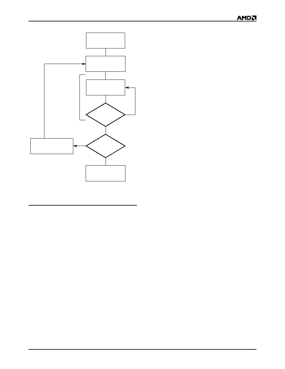
Note: See Table 5 for program command sequence.
Figure 2. Program Operation
Sector Erase Command Sequence
Sector erase is a six bus cycle operation. The sector
erase command sequence is initiated by writing two
unlock cycles, followed by a set-up command. Two ad-
ditional unlock write cycles are then followed by the ad-
dress of the sector to be erased, and the sector erase
command. Table 5 on page 19 shows the address and
data requirements for the sector erase command se-
quence.
The device does not require the system to preprogram
the memory prior to erase. The Embedded Erase algo-
rithm automatically programs and verifies the sector for
an all zero data pattern prior to electrical erase. The
system is not required to provide any controls or tim-
ings during these operations.
After the command sequence is written, a sector erase
time-out of 50 s begins. During the time-out period,
additional sector addresses and sector erase com-
mands may be written. Loading the sector erase buffer
may be done in any sequence, and the number of sec-
tors may be from one sector to all sectors. The time be-
tween these additional cycles must be less than 50 s,
otherwise the last address and command might not be
accepted, and erasure may begin. It is recommended
that processor interrupts be disabled during this time to
ensure all commands are accepted. The interrupts can
be re-enabled after the last Sector Erase command is
written. If the time between additional sector erase
commands can be assumed to be less than 50 s, the
system need not monitor DQ3. Any command other
than Sector Erase or Erase Suspend during the
time-out period resets the device to reading array
data. The system must rewrite the command sequence
and any additional sector addresses and commands.
The system can monitor DQ3 to determine if the sector
erase timer has timed out. (See “DQ3: Sector Erase
Timer” on page 22.) The time-out begins from the rising
edge of the final WE# pulse in the command sequence.
Once the sector erase operation has begun, only the
Erase Suspend command is valid. All other commands
are ignored. Note that a hardware reset during the
sector erase operation immediately terminates the op-
eration. The Sector Erase command sequence should
be reinitiated once the device has returned to reading
array data, to ensure data integrity.
When the Embedded Erase algorithm is complete, the
device returns to reading array data and addresses are
no longer latched. The system can determine the sta-
tus of the erase operation by using DQ7, DQ6, DQ2, or
RY/BY#. The Erase Resume command is valid only
during the Erase Suspend mode. See “Erase Sus-
pend/Erase Resume Commands” on page 17for infor-
mation on these status bits.
Figure 3, on page 18 illustrates the algorithm for the
erase operation. See Figure 3, on page 18 for parame-
ters, and to the Figure 12, on page 31 for timing wave-
forms.
Erase Suspend/Erase Resume Commands
The Erase Suspend command allows the system to in-
terrupt a sector erase operation and then read data
from, or program data to, any sector not selected for
erasure. This command is valid only during the sector
erase operation, including the 50 s time-out period
during the sector erase command sequence. The
Erase Suspend command is ignored if written during
the chip erase operation or Embedded Program algo-
rithm. Writing the Erase Suspend command during the
Sector Erase time-out immediately terminates the
time-out period and suspends the erase operation. Ad-
dresses are “don’t-cares” when writing the Erase Sus-
pend command.
When the Erase Suspend command is written during a
sector erase operation, the device requires a maximum
of 20 s to suspend the erase operation. However,
when the Erase Suspend command is written during
the sector erase time-out, the device immediately ter-
START
Write Program
Command Sequence
Data Poll
from System
Verify Data?
No
Yes
Last Address?
No
Yes
Programming
Completed
Increment Address
Embedded
Program
algorithm
in progress
相關(guān)PDF資料 |
PDF描述 |
|---|---|
| AM29F032B-75FC | 4M X 8 FLASH 5V PROM, 70 ns, PDSO40 |
| AM29F080-120SEB | 1M X 8 FLASH 5V PROM, 120 ns, PDSO44 |
| AM29F080-150EEB | 1M X 8 FLASH 5V PROM, 150 ns, PDSO40 |
| Am29F100B-120DGI | Hex Inverters 14-TSSOP -40 to 85 |
| Am29F100B-120DPC | Hex Inverters 14-TSSOP -40 to 85 |
相關(guān)代理商/技術(shù)參數(shù) |
參數(shù)描述 |
|---|---|
| AM29F032B75ED | 制造商:Advanced Micro Devices 功能描述: |
| AM29F032B-75EF | 制造商:Spansion 功能描述: 制造商:Spansion 功能描述:32M (4M X 8-BIT) 5V FLSH SCTR 制造商:Spansion 功能描述:IC, FLASH MEM, 32MBIT, 75NS, 40-TSOP, Memory Type:Flash - NOR, Memory Size:32Mbi |
| AM29F032B-75EF\\T | 制造商:Spansion 功能描述:32M (4MX8) 5V, UNIFORM SECTOR, TSOP40, IND, HAZMAT TR - Tape and Reel |
| AM29F032B-75EF\T | 制造商:Spansion 功能描述:32M (4MX8) 5V, UNIFORM SECTOR, TSOP40, IND, HAZMAT TR - Tape and Reel |
| AM29F032B-75SF | 功能描述:閃存 32M (4MX8) 75ns 5v Parallel NOR 閃存 RoHS:否 制造商:ON Semiconductor 數(shù)據(jù)總線寬度:1 bit 存儲(chǔ)類型:Flash 存儲(chǔ)容量:2 MB 結(jié)構(gòu):256 K x 8 定時(shí)類型: 接口類型:SPI 訪問時(shí)間: 電源電壓-最大:3.6 V 電源電壓-最小:2.3 V 最大工作電流:15 mA 工作溫度:- 40 C to + 85 C 安裝風(fēng)格:SMD/SMT 封裝 / 箱體: 封裝:Reel |
發(fā)布緊急采購,3分鐘左右您將得到回復(fù)。