- 您現(xiàn)在的位置:買賣IC網(wǎng) > PDF目錄92888 > AA038N2-00 28000 MHz - 40000 MHz RF/MICROWAVE WIDE BAND LOW POWER AMPLIFIER PDF資料下載
參數(shù)資料
| 型號: | AA038N2-00 |
| 元件分類: | 放大器 |
| 英文描述: | 28000 MHz - 40000 MHz RF/MICROWAVE WIDE BAND LOW POWER AMPLIFIER |
| 封裝: | CHIP |
| 文件頁數(shù): | 1/2頁 |
| 文件大小: | 134K |
| 代理商: | AA038N2-00 |
Alpha Industries, Inc. [781] 935-5150
Fax [617] 824-4579 Email sales@alphaind.com www.alphaind.com
1
Specifications subject to change without notice. 12/99A
28–40 GHz GaAs MMIC
Low Noise Amplifier
Features
I Single Bias Supply Operation (4.5 V)
I 3.8 dB Typical Noise Figure at 38 GHz
I 17 dB Typical Small Signal Gain
I 0.25 m Ti/Pd/Au Gates
I 100% On-Wafer RF, DC and Noise Figure
Testing
I 100% Visual Inspection to MIL-STD-883
MT 2010
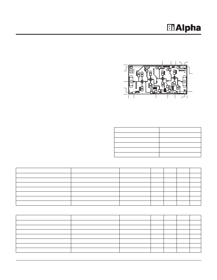
Chip Outline
AA038N1-00, AA038N2-00
Description
Alpha’s four-stage reactively-matched 28–40 GHz GaAs
MMIC low noise amplifier has typical small signal gain of
17 dB with a typical noise figure of 3.8 dB at 38 GHz. The
chip uses Alpha’s proven 0.25
m low noise PHEMT
technology, and is based upon MBE layers and electron
beam lithography for the highest uniformity and
repeatability. The FETs employ surface passivation to
ensure a rugged, reliable part with through-substrate via
holes and gold-based backside metallization to facilitate
a conductive epoxy die attach process.
Parameter
Condition
Symbol
Min.
Typ.3
Max.
Unit
Drain Current
IDS
35
50
mA
Small Signal Gain
F = 28–40 GHz
G
15
17
dB
Noise Figure
F = 38 GHz
NF
3.8
4.2
dB
Input Return Loss
F = 28–40 GHz
RLI
-10
-6
dB
Output Return Loss
F = 28–40 GHz
RLO
-8
-6
dB
Output Power at 1 dB Gain Compression1
F = 38 GHz
P1 dB
6
dBm
Thermal Resistance2
ΘJC
101
°C/W
Electrical Specifications at 25°C (VDS = 4.5 V)
AA038N1-00
Parameter
Condition
Symbol
Min.
Typ.3
Max.
Unit
Drain Current
IDS
35
50
mA
Small Signal Gain
F = 37–39.5 GHz
G
17
19
dB
Noise Figure
F = 38 GHz
NF
3.8
4.2
dB
Input Return Loss
F = 37–39.5 GHz
RLI
-14
-6
dB
Output Return Loss
F = 37–39.5 GHz
RLO
-11
-8
dB
Output Power at 1 dB Gain Compression1
F = 38 GHz
P1 dB
6
dBm
Thermal Resistance2
ΘJC
101
°C/W
AA038N2-00
1. Not measured on a 100% basis.
2. Calculated value based on measurement of discrete FET.
3. Typical represents the median parameter value across the specified
frequency range for the median chip.
0.000
0.588
0.246
1.264
1.813
2.146
2.710
2.600
0.087
0.124
1.355
1.560
1.961
2.183
2.445
2.599
1.267
1.274
Dimensions indicated in mm.
All DC (V) pads are 0.1 x 0.1 mm and RF In, Out pads are 0.07 mm wide.
Chip thickness = 0.1 mm.
Characteristic
Value
Operating Temperature (TC)
-55°C to +90°C
Storage Temperature (TST)
-65°C to +150°C
Bias Voltage (VD)6 VDC
Power In (PIN)
10 dBm
Junction Temperature (TJ)
175°C
Absolute Maximum Ratings
相關(guān)PDF資料 |
PDF描述 |
|---|---|
| AA038N1-00 | 28000 MHz - 40000 MHz RF/MICROWAVE WIDE BAND LOW POWER AMPLIFIER |
| AA038N3-00 | 37000 MHz - 40000 MHz RF/MICROWAVE WIDE BAND LOW POWER AMPLIFIER |
| AA100-59 | 750 MHz - 2000 MHz RF/MICROWAVE VARIABLE ATTENUATOR, 2.1 dB INSERTION LOSS-MAX |
| AA104-73 | 0.03 MHz - 2500 MHz RF/MICROWAVE VARIABLE ATTENUATOR, 1.3 dB INSERTION LOSS-MAX |
| AA104-73 | 0.03 MHz - 2500 MHz RF/MICROWAVE VARIABLE ATTENUATOR, 1.3 dB INSERTION LOSS-MAX |
相關(guān)代理商/技術(shù)參數(shù) |
參數(shù)描述 |
|---|---|
| AA038P1-00 | 制造商:SKYWORKS 制造商全稱:SKYWORKS 功能描述:36-39 GHz GaAs MMIC Driver Amplifier |
| AA038P2-00 | 制造商:ALPHA 制造商全稱:ALPHA 功能描述:37-40 GHz GaAs MMIC Driver Amplifier |
| AA038P5-00 | 制造商:ALPHA 制造商全稱:ALPHA 功能描述:37-39 GHz GaAs MMIC Power Amplifier |
| AA03A | 制造商:未知廠家 制造商全稱:未知廠家 功能描述:Analog IC |
| AA03A-005L-050S | 制造商:Emerson Network Power 功能描述: |
發(fā)布緊急采購,3分鐘左右您將得到回復(fù)。