- 您現(xiàn)在的位置:買賣IC網(wǎng) > PDF目錄24809 > 935263294551 (NXP SEMICONDUCTORS) 2 CHANNEL(S), 1M bps, SERIAL COMM CONTROLLER, PQFP44 PDF資料下載
參數(shù)資料
| 型號: | 935263294551 |
| 廠商: | NXP SEMICONDUCTORS |
| 元件分類: | 微控制器/微處理器 |
| 英文描述: | 2 CHANNEL(S), 1M bps, SERIAL COMM CONTROLLER, PQFP44 |
| 封裝: | 10 X 10 X 1.75 MM, PLASTIC, QFP-44 |
| 文件頁數(shù): | 13/48頁 |
| 文件大?。?/td> | 324K |
| 代理商: | 935263294551 |
第1頁第2頁第3頁第4頁第5頁第6頁第7頁第8頁第9頁第10頁第11頁第12頁當(dāng)前第13頁第14頁第15頁第16頁第17頁第18頁第19頁第20頁第21頁第22頁第23頁第24頁第25頁第26頁第27頁第28頁第29頁第30頁第31頁第32頁第33頁第34頁第35頁第36頁第37頁第38頁第39頁第40頁第41頁第42頁第43頁第44頁第45頁第46頁第47頁第48頁
Philips Semiconductors
Product specification
SC28L92
3.3V–5.0V Dual Universal Asynchronous
Receiver/Transmitter (DUART)
2000 Jan 21
20
MR1A[4:3]or MR1B[4:3] to ‘11’ for Channels A and B, respectively.
In this mode of operation, a ‘master’ station transmits an address
character followed by data characters for the addressed ‘slave’
station. The slave stations, with receivers that are normally disabled,
examine the received data stream and ‘wakeup’ the CPU (by setting
RxRDY)only upon receipt of an address character. The CPU
compares the received address to its station address and enables
the receiver if it wishes to receive the subsequent data characters.
Upon receipt of another address character, the CPU may disable the
receiver to initiate the process again.
A transmitted character consists of a start bit, the programmed
number of data bits, and Address/Data (A/D) bit, and the
programmed number of stop bits. The polarity of the transmitted A/D
bit is selected by the CPU by programming bit MR1A[2]/MR1B[2].
MR1A[2]/MR1B[2] = 0 transmits a zero in the A/D bit position, which
identifies the corresponding data bits as data while
MR1A[2]/MR1B[2] = 1 transmits a one in the A/D bit position, which
identifies the corresponding data bits as an address. The CPU
should program the mode register prior to loading the corresponding
data bits into the TxFIFO.
In this mode, the receiver continuously looks at the received data
stream, whether it is enabled or disabled. If disabled, it sets the
RxRDY status bit and loads the character into the RxFIFO if the
received A/D bit is a one (address tag), but discards the received
character if the received A/D bit is a zero (data tag). If enabled, all
received characters are transferred to the CPU via the RxFIFO. In
either case, the data bits are loaded into the data FIFO while the
A/D bit is loaded into the status FIFO position normally used for
parity error (SRA[5] or SRB[5]). Framing error, overrun error, and
break detect operate normally whether or not the receive is enabled.
PROGRAMMING
The operation of the DUART is programmed by writing control words
into the appropriate registers. Operational feedback is provided via
status registers which can be read by the CPU. The addressing of
the registers is described in Table 1.
The contents of certain control registers are initialized to zero on
RESET. Care should be exercised if the contents of a register are
changed during operation, since certain changes may cause
operational problems.
For example, changing the number of bits per character while the
transmitter is active may cause the transmission of an incorrect
character. In general, the contents of the MR, the CSR, and the
OPCR should only be changed while the receiver(s) and
transmitter(s) are not enabled, and certain changes to the ACR
should only be made while the C/T is stopped.
Each channel has 3 mode registers (MR0, 1, 2) which control the
basic configuration of the channel. Access to these registers is
controlled by independent MR address pointers. These pointers are
set to 0 or 1 by MR control commands in the command register
“Miscellaneous Commands”. Each time the MR registers are
accessed the MR pointer increments, stopping at MR2. It remains
pointing to MR2 until set to 0 or 1 via the miscellaneous commands
of the command register. The pointer is set to 1 on reset for
compatibility with previous Philips Semiconductors UART software.
Mode, command, clock select, and status registers are duplicated
for each channel to provide total independent operation and control.
Refer to Table 2 for register bit descriptions. The reserved registers
at addresses H‘02’ and H‘0A’ should never be read during normal
operation since they are reserved for internal diagnostics.
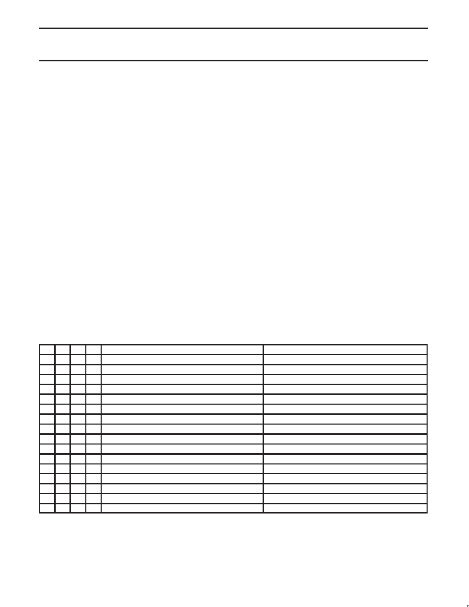
Table 1. SC28L92 register addressing READ (RDN = 0), WRITE (WRN = 0)
0
0
0
0
Mode Register A (MR0A, MR1A, MR2A)
Mode Register A (MR0A, MR1A, MR2A)
0
0
0
1
Status Register A (SRA)
Clock Select Register A (CSRA)
0
0
1
0
Reserved
Command Register A (CRA)
0
0
1
1
Rx Holding Register A (RxFIFOA)
Tx Holding Register A (TxFIFOA)
0
1
0
0
Input Port Change Register (IPCR)
Aux. Control Register (ACR)
0
1
0
1
Interrupt Status Register (ISR)
Interrupt Mask Register (IMR)
0
1
1
0
Counter/Timer Upper (CTU)
C/T Upper Preset Register (CTPU)
0
1
1
1
Counter/Timer Lower (CTL)
C/T Lower Preset Register (CTPL)
1
0
0
0
Mode Register B (MR0B, MR1B, MR2B)
Mode Register B (MR0B, MR1B, MR2B)
1
0
0
1
Status Register B (SRB)
Clock Select Register B (CSRB)
1
0
1
0
Reserved
Command Register B (CRB)
1
0
1
1
Rx Holding Register B (RxFIFOB)
Tx Holding Register B (TxFIFOB)
1
1
0
0
Interrupt vector (68K mode)
Interrupt vector (68K mode)
1
1
0
0
Misc. register (Intel mode), IVR Motorola mode
Misc. register (Intel mode), IVR Motorola mode
1
1
0
1
Input Port (IPR)
Output Port Conf. Register (OPCR)
1
1
1
0
Start Counter Command
Set Output Port Bits Command (SOPR)
1
1
1
1
Stop Counter Command
Reset output Port Bits Command (ROPR)
NOTE:
1. The three MR registers are accessed via the MR Pointer and Commands 0x1n and 0xBn (where n = represents receiver and transmitter enable bits)
相關(guān)PDF資料 |
PDF描述 |
|---|---|
| 935263293518 | 2 CHANNEL(S), 1M bps, SERIAL COMM CONTROLLER, PQCC44 |
| 935263294528 | 2 CHANNEL(S), 1M bps, SERIAL COMM CONTROLLER, PQFP44 |
| 07LC-10T050 | ISOLATED DC/DC CONVERTERS 48V Input / 5V/2A or 12V/1A or 24V/0.5A Output |
| 07LC-10T120 | ISOLATED DC/DC CONVERTERS 48V Input / 5V/2A or 12V/1A or 24V/0.5A Output |
| 07LC-10T240 | ISOLATED DC/DC CONVERTERS 48V Input / 5V/2A or 12V/1A or 24V/0.5A Output |
相關(guān)代理商/技術(shù)參數(shù) |
參數(shù)描述 |
|---|---|
| 935264217557 | 制造商:NXP Semiconductors 功能描述:SUB ONLY IC |
| 935267356112 | 制造商:NXP Semiconductors 功能描述:IC TEA1507PN |
| 935268081112 | 制造商:NXP Semiconductors 功能描述:SUB ONLY IC |
| 935268721125 | 制造商:NXP Semiconductors 功能描述:Buffer/Line Driver 1-CH Non-Inverting 3-ST CMOS 5-Pin TSSOP T/R |
| 935269304128 | 制造商:ST-Ericsson 功能描述:IC AUDIO CODEC W/TCH SCRN 48LQFP |
發(fā)布緊急采購,3分鐘左右您將得到回復(fù)。